

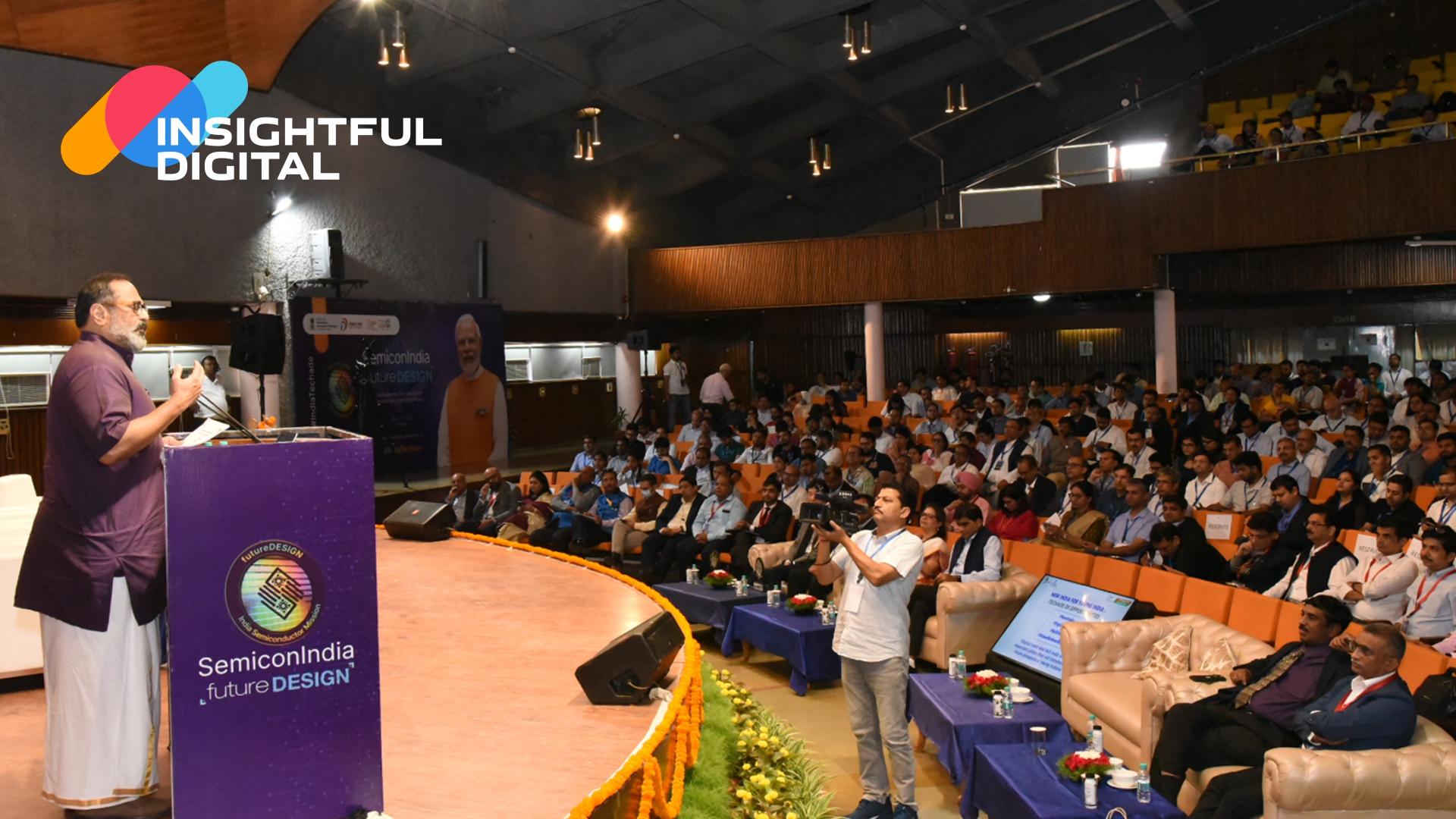
In a significant event held at the Vikram Sarabhai Space Centre (VSSC) in Kerala, Union Minister Rajeev Chandrasekhar, responsible for Electronics and IT, Skill Development and Entrepreneurship, and Jal Shakti, expressed India's potential to become a global semiconductor hub. Chandrasekhar emphasized the necessity of designing chips and IP for diverse industries and outlined a roadmap for entrepreneurs in Trivandrum and Kerala to lead the innovation drive.
Leading Semiconductor Design Infrastructure
At the heart of this vision is the ChipIN Centre, a revolutionary facility poised to transform semiconductor design in India. Offering diverse design flows and cutting-edge tools, ChipIN aims to democratize access to chip design infrastructure across the country. With a focus on advanced node technologies, the center seeks to empower students, researchers, and industry professionals with the resources needed to foster innovation.
Empowering India's Semiconductor Ecosystem
Centralized Design Facility: The ChipIN Centre serves as a centralized hub, offering a wide range of design flows and services to the semiconductor community in India.
Advanced Tools: It hosts state-of-the-art tools covering the entire chip design cycle, including front-end design, back-end design, PCB design, and analysis, catering to various design types.
Accessibility: The center aims to make chip design infrastructure easily accessible to the semiconductor community, promoting inclusivity and collaboration.
Comprehensive Support: ChipIN Centre provides comprehensive support, offering services for design fabrication and packaging, ensuring a seamless design process.
Educational Outreach: Engaging with over 10,000 students from 120 academic institutions and 20 startups, ChipIN aims to empower the next generation of semiconductor engineers through access to cutting-edge Electronic Design Automation (EDA) tools.
Expansion Plans: With plans to empower 85,000 students across various academic levels, the ChipIN Centre aims to foster a culture of innovation and skill development throughout the country.
Industry Collaboration: ChipIN collaborates with industry leaders to support academia and startups, enhancing access to EDA tools and expertise.
Government Support: Aligned with the government's vision, the ChipIN Centre receives support to strengthen the semiconductor ecosystem in India, driving towards Prime Minister Narendra Modi's goal of making India a global semiconductor hub.
India's Journey Towards Global Semiconductor Leadership
As India progresses towards global semiconductor prominence, initiatives like the ChipIN Centre and government-supported assistance programs are set to ignite innovation and entrepreneurship in semiconductor design. With visionary leadership, industry collaboration, and a robust innovation ecosystem, India is poised to lead in shaping the future of technology.
Objective Questions for Competitive Exams
Q.1. What is the primary focus of the ChipIN Centre?
a) Manufacturing semiconductors
b) Designing semiconductor chips and IP
c) Training astronauts
Answer: b) Designing semiconductor chips and IP
Q.2. Where was the ChipIN Centre launched?
a) Delhi
b) Mumbai
c) Kerala
Answer: c) Kerala
Q.3. Who is the Union Minister responsible for launching the ChipIN Centre?
a) Nirmala Sitharaman
b) Rajeev Chandrasekhar
c) Piyush Goyal
Answer: b) Rajeev Chandrasekhar
Q.4. What is the aim of the ChipIN Centre in terms of accessibility?
a) To make semiconductor manufacturing cheaper
b) To make chip design infrastructure easily accessible
c) To provide training in software development
Answer: b) To make chip design infrastructure easily accessible
Q.5. How many students does the ChipIN Centre plan to empower across various academic levels?
a) 10,000
b) 50,000
c) 85,000
Answer: c) 85,000
Q.6. What is the ultimate goal of the ChipIN Centre and government-supported initiatives?
a) To make India a global semiconductor hub
b) To develop new software technologies
c) To train more IT professionals
Answer: a) To make India a global semiconductor hub